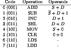
Table: Function Code and Its Implementation by an Adder
There are only eight DIP switches available on our FPGA prototype board, of which, three are used for specifying the operations. Hence four DIP switches for specifying data to be loaded into registers are shared among S and D-registers. Also one push-button switch is used for generation of manual-clock signal.
First, operations (including LOAD to S and D-registers) are coded into 3-bit numbers and their operands are chosen so that they can be achieved by a 4-bit adder (X74-83).

Table: Function Code and Its Implementation by an Adder
To give the adder proper operands, the following circuits are used:
 (bit-complement) +1 to D.
The signals in Table 0.3 are generated from the function code specified by DIP switches to control datapath.
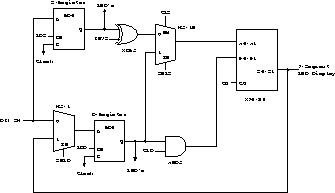
With break-down of the datapath given by now, we can write the block diagram shown in Figure 0.1. A thicker line it the block diagram represents 4-bit data signals, and four instances of macro are used in parallel except X74-83. Note that Figure 0.1 shows only the part manipulating data, i.e. control signal generation part (Decoder X74-138 and some random logic were used) and I/O parts are not included.

Figure: Block Diagram of the Datapath