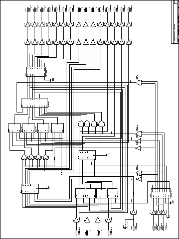
The design was captured in a schematic by OrCAD as shown in
Figure 0.2, and then compiled into a Xilinx LCA file.
Correctness of the design was confirmed as follows:
Load S and D-registers with the value of DIP switches,
and they were displayed on 4-LED's.
Arithmetic and logical operations worked and were displayed
on 7-segments LED correctly.
Outputs from the adder are written to D-register.
Figure: Schematic
Hitoshi Oi All Rights Reserved
Fri Dec 22 00:18:12 EST 1995