Schematic of the 4bit adder is shown in Figure 0.1.
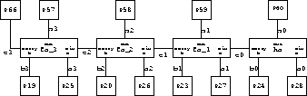
Figure 0.1: 4bit Ripple Carry Adder Schematic
Four LCB's (one for each bit) are used for main functionality of the adder, and they are given names ha, fa_1, fa_2, and fa_3 from LSB to MSB. Signal wires are named as shown in the figure. Sum and carry are generated by LCB's F and G functional blocks respectively. Two 4bit inputs are given by DIP switches, and 5bit output (4bit sum and 1bit over-flow) are given to LEDs. These signals are connected to LCB's via I/O blocks.
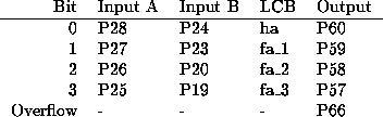
The following table gives LCB's and I/O blocks used for each bit: