Since a CLB contains two FF's, it looks like that we can implement
two bits with one CLB. However their clock signals are not
independent (we have choice of only clock and  for clock input of each FF)
we need one CLB for each bit in a ripple counter
(Figure 0.2).
for clock input of each FF)
we need one CLB for each bit in a ripple counter
(Figure 0.2).
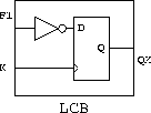
To build a T-FF, we used a D-FF (on X-side) and F-function block of the CLB. F-function block is used as an inverter; its output is the complement of F1 input. QX pin is fed back to F1 so that the next value of the FF will be toggled at each falling edge of the clock signal (K input)
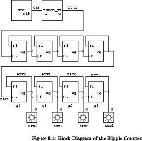
The Figure 0.3 shows the block diagram of the ripple counter, with the name of CLB's, signals, and I/O blocks. The counter has total length of 8bits, and last 4bits are connected to LED's to see its operation. The first 4bits are used as ``pre-scaler'' to slow down the speed of LED flashing. The block OSC, which is the built-in RC oscillator, is the source of clock signal. It provides various frequency of signals, from 8MHz to 15Hz, and we used the lowest one, 15Hz. It is buffered by the block BUFGS, and then connected to the first bit of the ripple counter through the secondary global net.